2D interfaces in future transistors
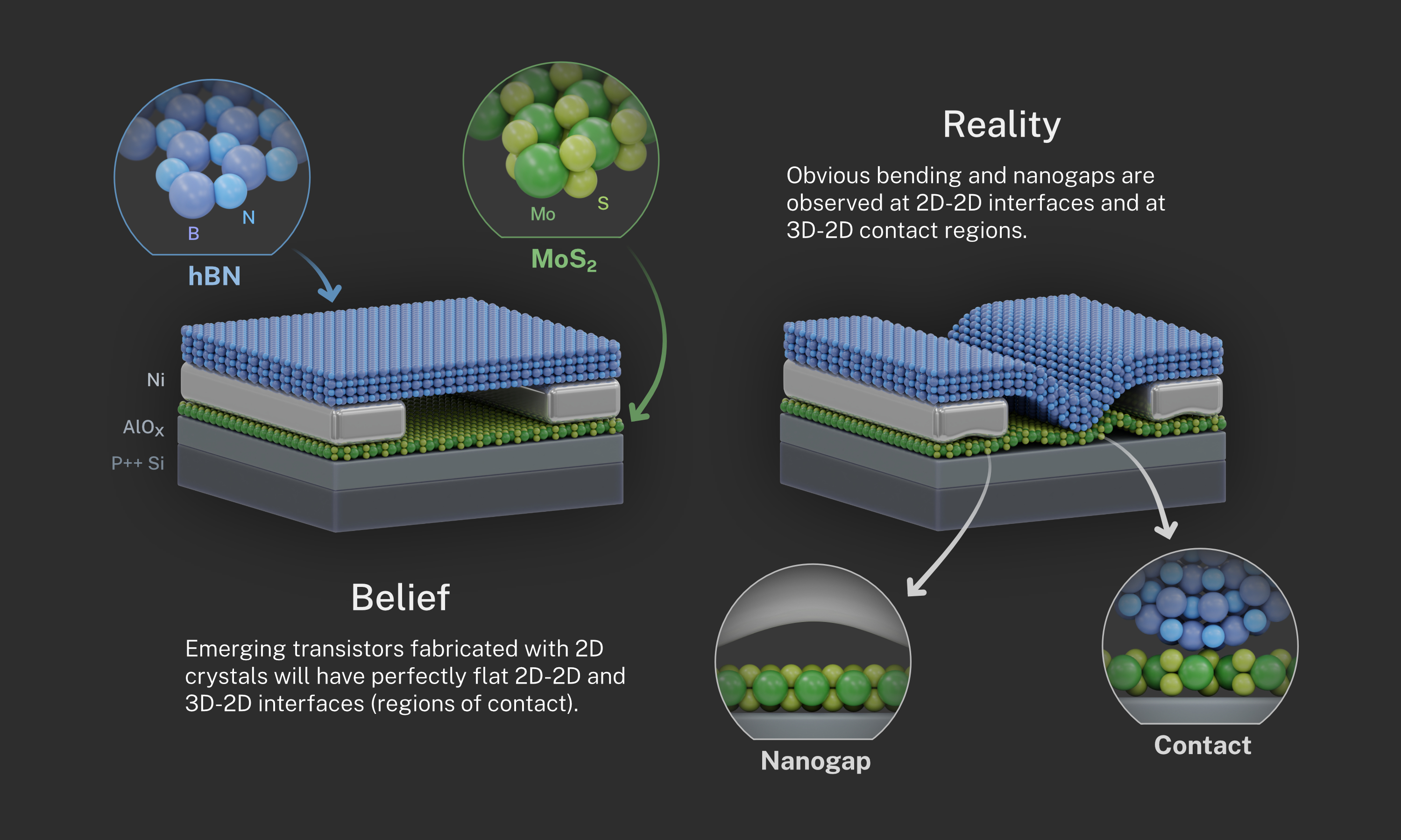
- Researchers generally expect that transistors fabricated with 2D crystals will have perfectly flat 2D-2D and 3D-2D interfaces (regions of contact). But new evidence shows that in reality, there are obvious bending and nanogaps at these interfaces.
- Client
- NIST
- Date
- June 2022
- Categories
- Illustration Diagram
- Link
- https://www.nist.gov/news-events/news/2022/06/road-tiny-transistors-how-flat-flat
Project Notes
I created an supplementary image to show the difference between a traditional MOSFET vs. a 2D FET: