Detecting transistor defects
- A four-panel cartoon describing a new NIST technique for characterizing interface defects in a transistor material.
- Client
- NIST
- Date
- October 2021
- Categories
- Diagram
- Link
- https://www.nist.gov/news-events/news/2021/10/nist-collaborators-develop-sensitive-new-way-detecting-transistor-defects
Project Notes
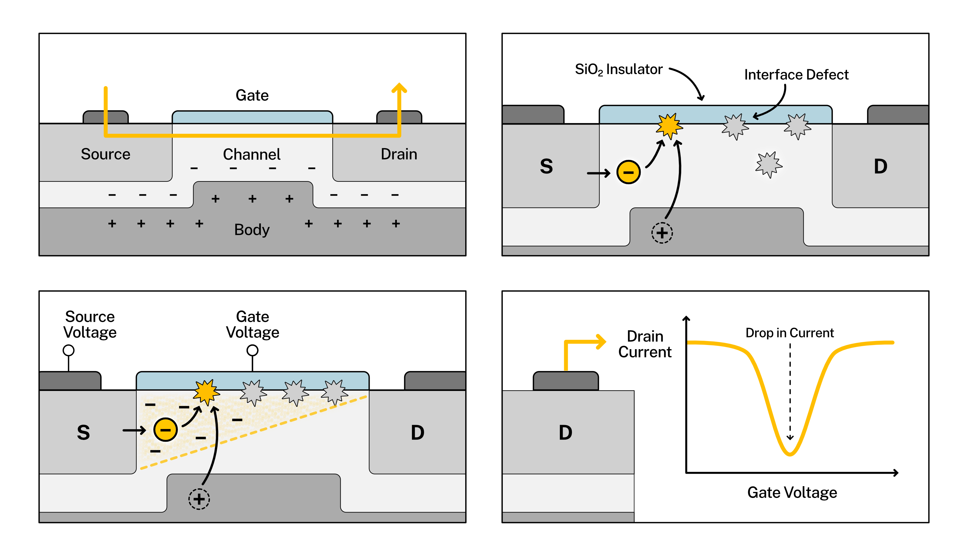
The captions for the cartoon are as follows:
- During normal transistor operation, a conductive channel (controlled by the gate) forms between the source and drain, allowing a current to flow.
- However, electrons moving from the source to the drain can encounter defects that lead to recombination with a hole, resulting in a loss of current and making the transistor unreliable. The most important of these are called interface defects, existing at the interface between the silicon oxide and silicon layers.
- In order to count these defects, researchers place the transistor into “bipolar amplification” mode by applying a voltage to the source and gate. This creates a decreasing concentration of electrons across the channel. In this configuration, the current from the source to the drain is highly sensitive to interface defects.
- By monitoring the current at the drain while varying the gate voltage, researchers can accurately determine the number of defects from the change in the current.