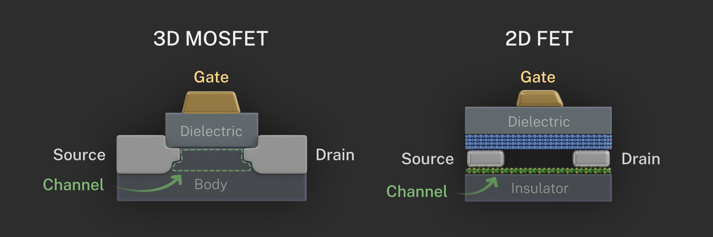
2D interfaces in future transistors
- Client
- NIST
- Year
- 2022
- Type
- explanatory diagram
- Field
- nanoelectronics / transistor materials
- Links
- NIST news
- Description
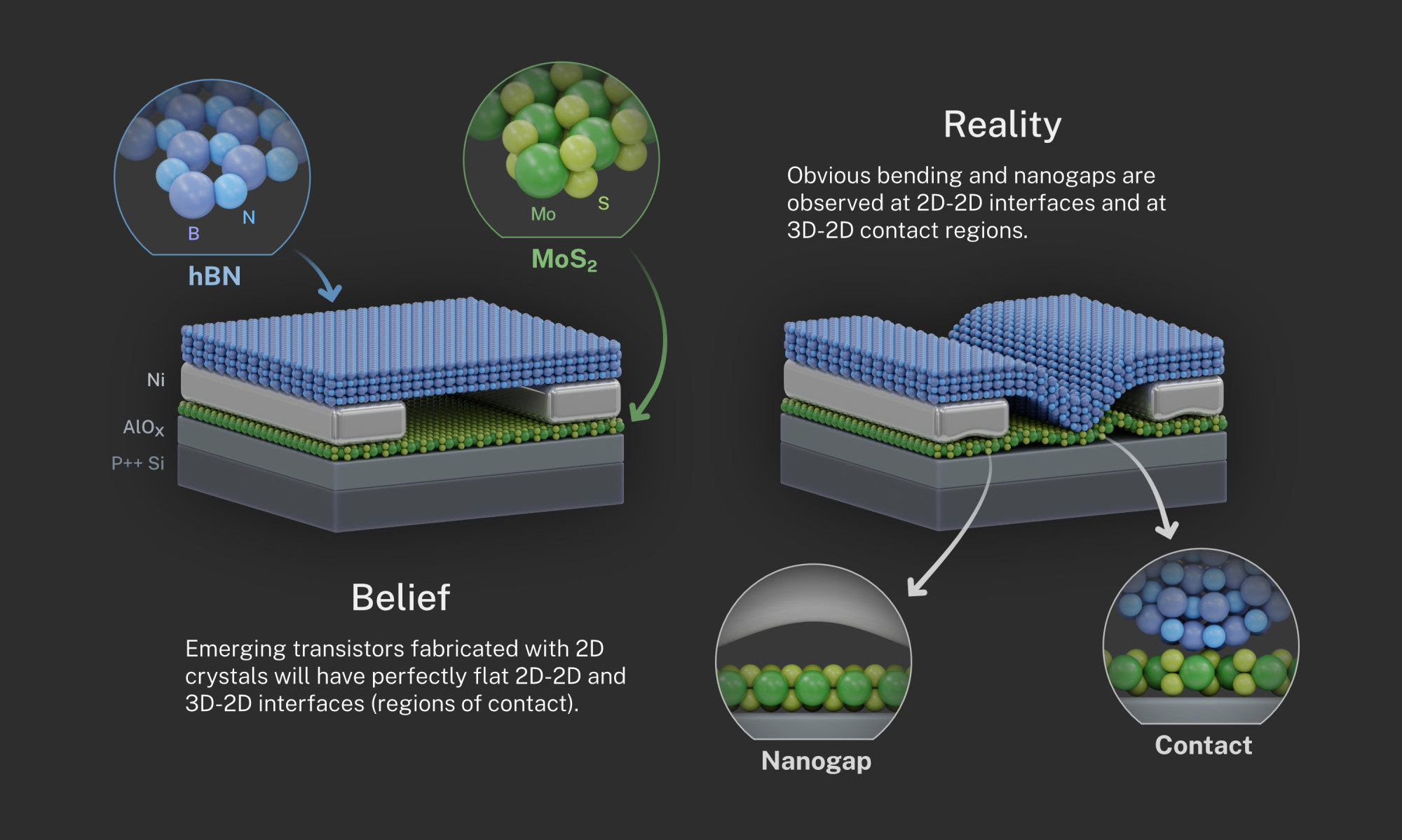
- Diagram comparing the flat interfaces researchers hoped for in 2D transistors with the bent layers and nanogaps found in measurements.
Context
The story explained why atomically thin materials are attractive for future transistors, and why the interfaces between those materials matter. Measurements showed that the layers were not as flat as expected; they bent and left nanometer-scale gaps where the materials met.
Approach
The image puts the ideal structure next to the measured structure, then places that comparison back into the transistor stack. The main job was to make the mismatch between expectation and measurement visible immediately.