Universal visible emitters in nanoscale integrated photonics
- Client
- NIST
- Year
- 2023
- Type
- explanatory diagram
- Field
- integrated photonics / nanophotonics
- Links
- NIST news / Optica paper
- Description
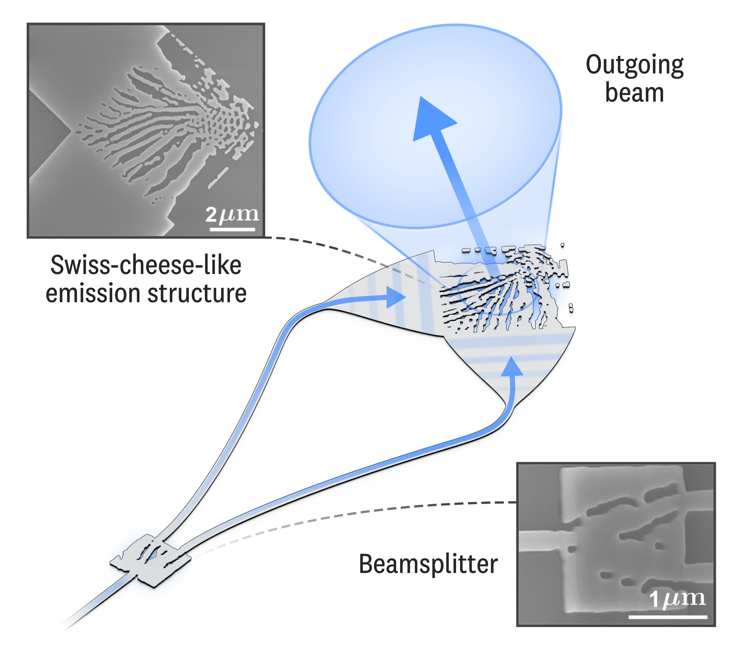
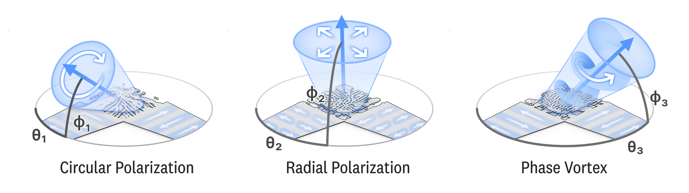
- Two public-facing diagrams showing how a nanoscale photonic chip transforms a single incoming beam into multiple outgoing beams with controlled polarization and phase.
Context
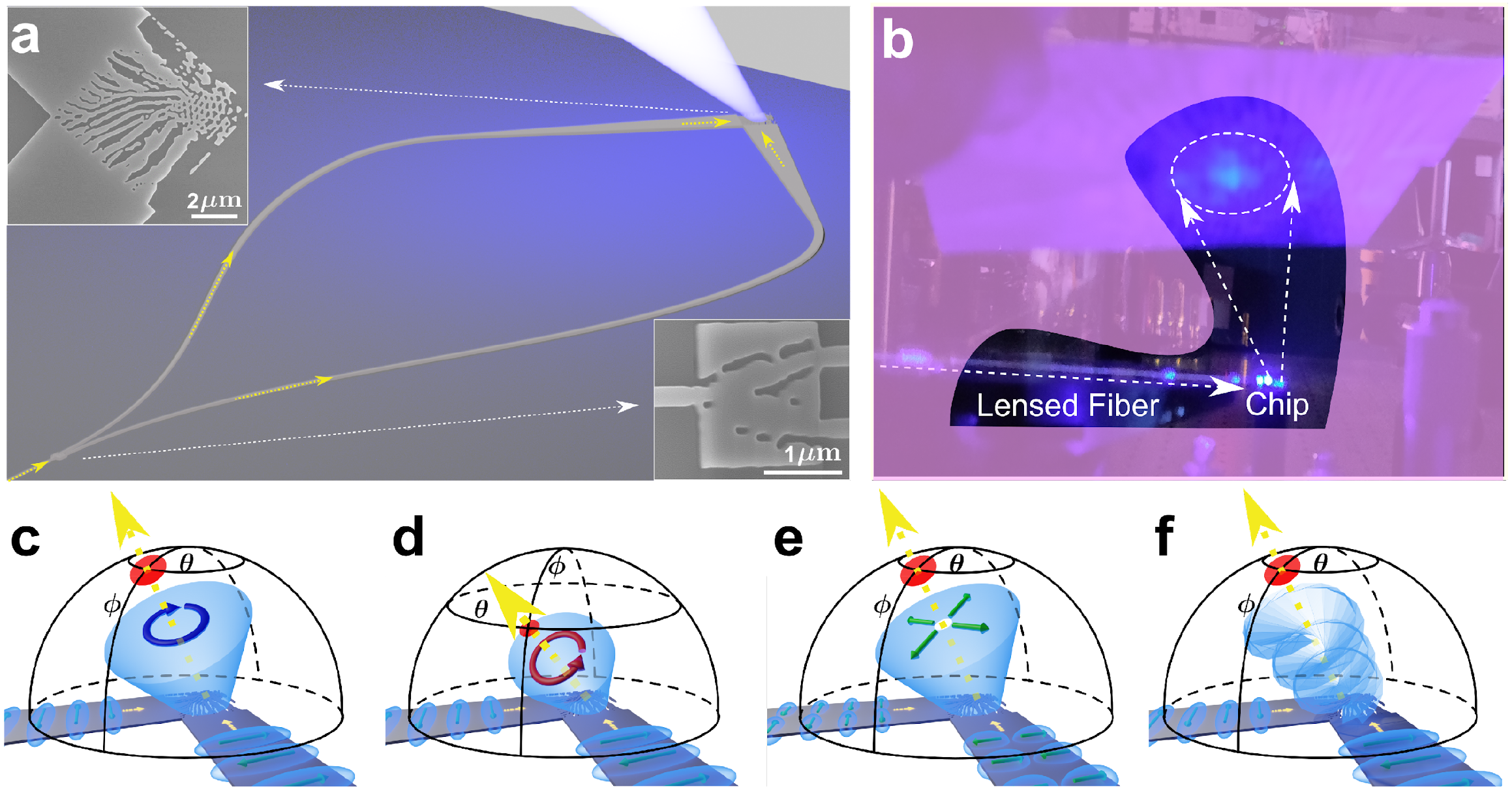
The figures accompanied a NIST news article about a photonic chip designed to convert one input beam into multiple visible-light beams. The source paper contained a dense multi-panel figure combining microscope images, optical paths, device geometry, and phase/polarization examples.
Approach
The original figure combined several technical views, image sources, colors, and perspective systems, which made the mechanism difficult to read quickly outside the paper context. I used the original SEM images to recreate the waveguide surface patterns in Blender, then redrew the device, beam paths, polarization states, and callouts using restrained blue, white, and black.